Nano-Structured GeSn Coatings for Photonics – GESNAPHOTO_M-ERA.NET project
Project Director: Dr. Toma STOICA
The project has as a main objective the manufacturing of nano-structured GeSn films for optical detection and light emission in the short-wave infrared (SWIR) range. The novelty of the project consists in nano-structuring of layers containing GeSn in order to create GeSn quantum dots (nano-crystals) for increased sensitivity. GeSn is a new group IV advanced coating material based on alloying Ge and Sn elements which extends the IR photonic range of Ge. The most important property is the transition into direct bandgap semiconductor for moderate Sn concentration, of critical importance for photonics of group IV semiconductors. Thus, the project deals with an alternative solution to the present III-V IR technology, a solution which is less expensive, environmentally friendly and compatible with Si technology. The IR detection has many practical applications as for example night vision, medical applications, automotive, aviation, etc.
The main objectives of the project are:
- Obtaining functionalized coatings (films and multilayers) with nano-structured GeSn;
- Optical and electrical properties tuning for detection and emission in SWIR;
- Manufacture of demonstrators with optimized parameters.
![]()


![]()
![]()

The project will be accomplished by the consortium formed of: National Institute of Materials Physics – Romania (Project Coordinator, P1); National Institute for Research and Development in Optoelectronics – INOE 2000 – Romania (P2); Forschungszentrum Jülich, Peter Grünberg Institute (PGI-9) -Germany (P3) and companies OPTOELECTRONICA-2001 S.A – Romania (P4) and nanoplus Nanosystems and Technologies GmbH -Germany (P5).
Coordinator: National Institute of Materials Physics, NIMP - Romania
Project Coordinator: Dr. Toma Stoica
Partner: National Institute for Research and Development in Optoelectronics
Responsible of INOE-2000: Dr. Mariana Braic
Partner: Forschungszentrum Jülich, Peter Grünberg Institute - Geramany
Responsible of PGI-9: Prof. Detlev Grützmacher
Partner: OPTOELECTRONICA- 2001 S.A - Romania
Responsible of OPTOEL: Dr. Alexandra Enuica
Partner: nanoplus Nanosystems and Technologies GmbH - Germany
Responsible of nanoplus: Dr. Johannes Koeth
![]()
![]()
![]()
![]()
11-06-2019 EuroNanoForum-Bucharest_12-14.06.2019-GeSn_Gesnaphoto, download pdf
03-06-2019 Agenda project GESNAPHOTO-Magurele-Buccharest 11_06_2019
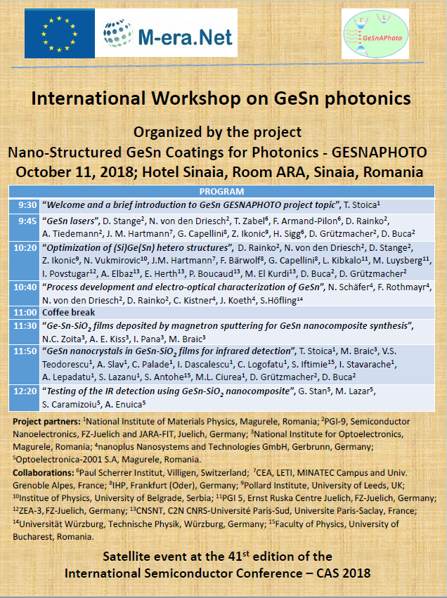
03-10-2018 International Workshop on GeSn photonics, Sinaia, 11-10-2018 download pdf
10-08-2018 Agenda project GESNAPHOTO-Magurele-Buccharest 20_07_2018
20-11-2017 Agenda project GESNAPHOTO-meeting PGI-9 FZ Juelich 09_11_2017
04-05-2017 Agenda_GESNAPHOTO_project_meeting_nanoplus_04_05_2017_0
14-11-2016 M.ERANET-3107-GESNAPHOTO Kick-off meeting Agenda -Kick_off-GESNAPHOTO
![]()
![]()
![]()
![]()
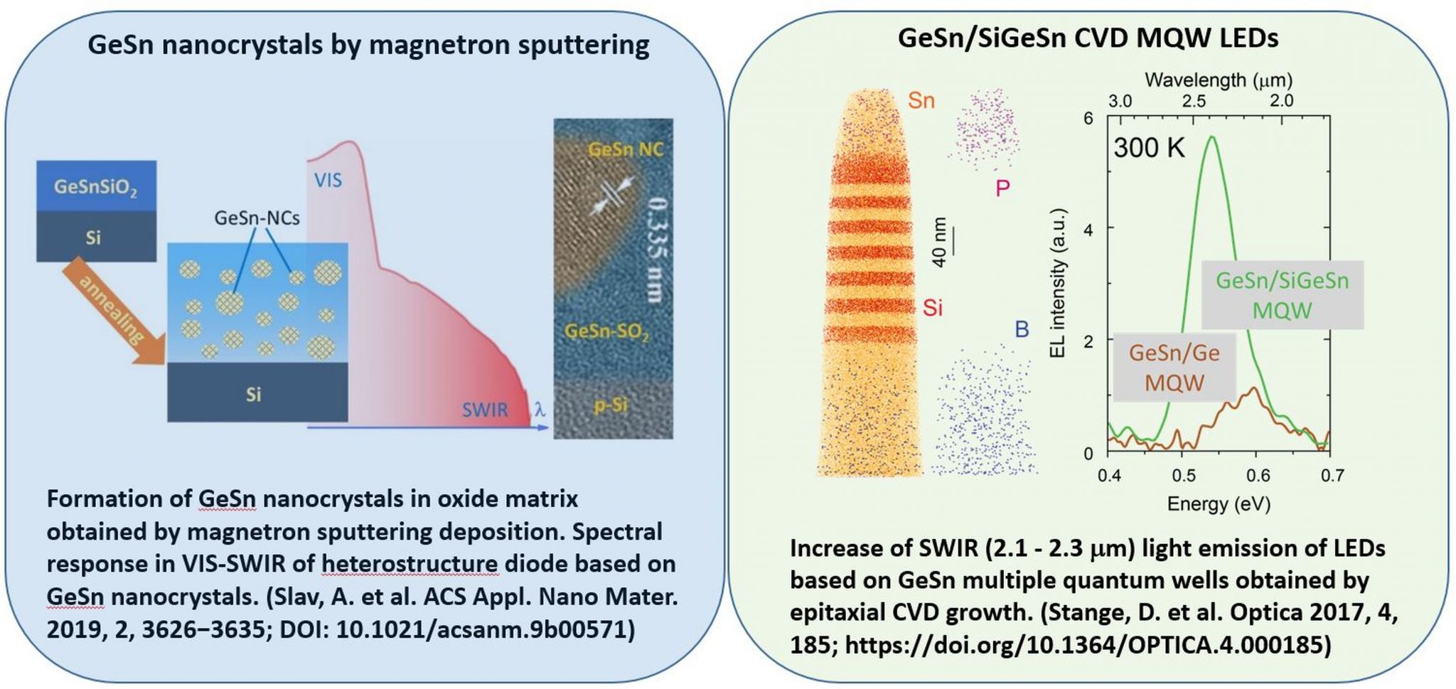
GeSn is a new semiconductor material for detection and emission in short-wave infrared (SWIR) light. The (Si)GeSn alloys offer an alternative solution to the current III-V IR technology, being less expensive, environmentally friendly and compatible with Si technology. GeSn is a direct-bandgap semiconductor, opening a new path for silicon photonics. The performances of the GeSn based devices can be enhanced by nano-structuring. This is the topic of the GESNAPHOTO project* in the frame of the M-ERA.NET EU program. The project is a synergistic partnership of research institutes and manufacturing companies from Romania and Germany. Two methods for fabrication of GeSn layers are addressed: cost effective magnetron sputtering (MS) and industrial standard chemical vapor (CVD) depositions. Multiple structural and topological characterization methods available in consortium as well and electronic band structure modeling are used. SWIR detection up to wavelength of 2.4 mm was demonstrated for GeSn nanocrystals (NCs) embedded in SiO2 obtained by MS deposited layers and light emission at about 2.5 µm on multiple quantum well and strained structures. Electroluminescence diodes and SWIR detectors were fabricated by using both homojunction and nanostructured multilayers of epitaxially grown (Si)GeSn on Ge-virtual substrates.
GESNAPHOTO-Stage IV Obtaining optoelectronic demonstrators based on nanostructured GeSn and functional testing
GESNAPHOTO-Stage III Multilayer structures based on GeSn nanocrystals for optoelectronic demonstrators
GESNAPHOTO-Stage II Optimization of nanostructured GeSn coatings and advanced characterizations
GESNAPHOTO-Stage I Obtaining nanostructured GeSn coatings and preliminary characterizations
![]()
![]()
![]()
![]()
Papers published/for publication in ISI journals:
- Short-wave infrared LEDs from GeSn/SiGeSn multiple quantum wells. D. Stange, N. von den Driesch, D. Rainko, S. Roesgaard, I. Povstugar, J.-M. Hartmann, T. Stoica, Z. Ikonic, S. Mantl, D. Grützmacher, and D. Buca, Optica 2017, 4, 185.
- SiGeSn Ternaries for Efficient Group IV Heterostructure Light Emitters. N. von den Driesch, D. Stange, S. Wirths, D. Rainko, I. Povstugar, A. Savenko, U. Breuer, R. Geiger, H. Sigg, Z. Ikonic, J.-M. Hartmann, D. Grützmacher, S. Mantl, and D. Buca, small 2017, 1603321.
- "Influence of preparation conditions on structure and photosensing properties of GeSi/TiO2 multilayers", A. Slav, C. Palade, I. Stavarache, V.S. Teodorescu, M.L. Ciurea, R. Müller, A. Dinescu, M.T. Sultan, A. Manolescu, J.T. Gudmundsson, H.G. Svavarsson, IEEE International Semiconductor Conference - CAS Proceedings (2017), pp. 63–66.
- "Photosensitive GeSi/TiO2 multilayers in VIS-NIR", C. Palade, I. Dascalescu, A. Slav, A.M. Lepadatu, S. Lazanu, T. Stoica, V.S. Teodorescu, M.L. Ciurea, F. Comanescu, R. Müller, A. Dinescu, A. Enuica, IEEE CAS Proceedings (2017), pp. 67–70.
- "Dense Ge nanocrystals embedded in TiO2 with exponentially increased photoconduction by field effect”, A.-M. Lepadatu, A. Slav, C. Palade, V.S. Teodorescu, M. Enculescu, S. Iftimie, S. Lazanu, M.L. Ciurea, T. Stoica, Scientific Reports (2018) 8:4898 DOI:10.1038/s41598-018-23316-3.
- „Optoelectric charging-discharging of Ge nanocrystals in floating gate memory”, C. Palade, A. Slav, A.M. Lepadatu, A.V. Maraloiu, I. Dascalescu, S. Iftimie, S. Lazanu, M.L. Ciurea, and T. Stoica, Appl. Phys. Lett. (2018) 113, 213106, doi: 10.1063/1.5039554 .
- „Enhanced photocurrent in GeSi NCs/TiO2 multilayers”, C. Palade, A. Slav, O. Cojocaru, V.S. Teodorescu, S. Lazanu, T. Stoica, M.T. Sultan, H.G. Svavarsson, M.L. Ciurea, IEEE CAS Proceedings (2018), pp. 73–76.
- „Enhanced photoconductivity of SiGe-trilayer stack by retrenching annealing conditions”, M.T. Sultan, J.T. Gudmundsson, A. Manolescu, M.L. Ciurea, C. Palade, A. V. Maraloiu, H.G. Svavarsson, IEEE CAS Proceedings (2018), pp. 61–64.
- „The effect of H2/Ar plasma treatment over photoconductivity of SiGe nanoparticles sandwiched between silicon oxide matrix”, M.T. Sultan, J.T. Gudmundsson, A. Manolescu, M.L. Ciurea, H.G. Svavarsson, IEEE CAS Proceedings (2018), pp. 257–260.
- “Advanced GeSn/SiGeSn Group IV Heterostructure Lasers”, N, von den Driesch, D. Stange, D. Rainko, I. Povstugar, P. Zaumseil, G. Capellini, T. Schröder, T. Denneulin, Z. Ikonic, J.-M. Hartmann, H. Sigg, S. Mantl, D. Grützmacher, and D. Buca, Adv. Sci. 2018, 5, 1700955, DOI: 10.1002/advs.201700955.
- “Investigation of carrier confinement in direct bandgap GeSn/SiGeSn 2D and 0D heterostructures”, D, Rainko, Z. Ikonic, N. Vukmirović, D. Stange, N. von den Driesch, D. Grützmacher, Dan Buca, Scientific Reports (2018) 8:15557, DOI:10.1038/s41598-018-33820-1.
- „GeSn nanocrystals in GeSnSiO2 layers obtained by magnetron sputtering for SWIR detection”, A. Slav, C. Palade, C.Logofatu, I. Dascalescu, A. M. Lepadatu, I. Stavarache, S. Iftimie, S. Antohe, S. Lazanu, V. S. Teodorescu, D. Buca, M. L. Ciurea, M. Braic, T. Stoica, ACS Applied Nano Materials (2019), 2. 3626, DOI: 10.1021/acsanm.9b00571.
Conference papers:
- “Nanocrystals of GeSn alloys in oxide matrix for optoelectronic applications”, I. Stavarache, A. Slav, M. Braic, V. S. Teodorescu, P. Prepelita, C. Palade, A.-M. Lepadatu, S. Lazanu, M. L. Ciurea, D. Stange, D. Buca, T.Stoica, Applied Nanotechnology And Nanoscience International Conference - ANNIC2017, Oct 18-20, 2017-Rome (oral presentation)
- "Influence of preparation conditions on structure and photosensing properties of GeSi/TiO2 multilayers", A. Slav, C. Palade, I. Stavarache, V.S. Teodorescu, M.L. Ciurea, R. Müller, A. Dinescu, M.T. Sultan, A. Manolescu, J.T. Gudmundsson, H.G. Svavarsson, IEEE International Semiconductor Conference - CAS 2017, October 11-14, Sinaia (oral presentation)
- "Photosensitive GeSi/TiO2 multilayers in VIS-NIR", C. Palade, I. Dascalescu, A. Slav, A.M. Lepadatu, S. Lazanu, T. Stoica, V.S. Teodorescu, M.L. Ciurea, F. Comanescu, R. Müller, A. Dinescu, A. Enuica, IEEE International Semiconductor Conference - - CAS 2017, October 11-14, Sinaia (oral presentation)
- "Ge nanocrystals in oxides with memory and photoelectrical properties", C. Palade, A. Slav, A.-M. Lepadatu, A.V. Maraloiu, S. Lazanu, C. Logofatu, T. Stoica, V.S. Teodorescu, M.L. Ciurea, The 9th International Conference on Advanced Materials - ROCAM 2017, July 11-14, Bucuresti (oral presentation)
- “Nanocrystals of GeSn alloys in oxide matrix for optoelectronic applications”, I. Stavarache, A. Slav, M. Braic, V. S. Teodorescu, P. Prepelita, C. Palade, A.-M. Lepadatu, S. Lazanu, M. L. Ciurea, D. Stange, D. Buca, T.Stoica, Applied Nanotechnology And Nanoscience International Conference - ANNIC2017, Oct 18-20, 2017-Rome (oral presentation).
- “Ge1-xSnx nanocrystal formation in (Ge1-xSnx)1-y(SiO2)y layers obtained by sputtering deposition”, T. Stoica, M. Braic, V.S. Teodorescu, A. Slav, C. Palade, I. Stavarache, M.P. Prepelita, A. Lepadatu, S. Lazanu, M.L. Ciurea, I. Povstugar, D. Stange, D. Grützmacher, D. Buca, proceedings pp.119–120, 1st Joint ISTDM/ICSI 2018 Conference – Potsdam, May 27-31, (oral presentation).
- "GeSn nanocrystals in GeSn-SiO2 composite films obtained by magnetron sputtering deposition”, A. Slav, M. Braic, V.S. Teodorescu, C. Palade, A. Lepadatu, I. Stavarache, M.P. Prepelita, C Logofatu, S. Lazanu, M.L. Ciurea, T. Stoica, EXMATEC 2018 – IMT, Bucharest, (oral presentation).
- „Physical parameters of trilayer structures in fg memory based on Ge NCs”, C. Palade, A. Slav, A.-M. Lepădatu, I. Stăvărache, I. Dăscălescu, S. Lazanu, T. Stoica, V. S. Teodorescu, M. L. Ciurea, IBWAP 2018-Constanta, (oral presentation).
- „Enhanced photocurrent in GeSi NCs/TiO2 multilayers”, C. Palade, A. Slav, O. Cojocaru, V.S. Teodorescu, S. Lazanu, T. Stoica, M.T. Sultan, H.G. Svavarsson, M.L. Ciurea, IEEE International Semiconductor Conference - CAS 2018, October 10-12, Sinaia (oral presentation).
- „Enhanced photoconductivity of SiGe-trilayer stack by retrenching annealing conditions”, M.T. Sultan, J.T. Gudmundsson, A. Manolescu, M.L. Ciurea, C. Palade, A. V. Maraloiu, H.G. Svavarsson, IEEE International Semiconductor Conference - CAS 2018, October 10-12, Sinaia (oral presentation).
- “The effect of H2/Ar plasma treatment over photoconductivity of SiGe nanoparticles sandwiched between silicon oxide matrix”, M.T. Sultan, J.T. Gudmundsson, A. Manolescu, M.L. Ciurea, H.G. Svavarsson, IEEE International Semiconductor Conference - CAS 2018, October 10-12, Sinaia (oral presentation).
- “Magnetron sputtering growth of epitaxial GeSn films on Ge buffered Si wafers”, N.C. Zoita, I. Pana, A. Kiss, I. Dascalescu, A. Slav, O. Muresan, C. Palade, D. Buca, T. Stoica, M.Braic, E-MRS May 27 - 31, 2019, Nice, France (poster).
- “GeSnSiO2 layers with embedded GeSn nanocristals for sensing in SWIR”, A. Slav, C. Palade, C. Logofatu, I. Dascalescu, A.M. Lepadatu, I. Stavarache, S. Iftimie, V. Braic, S. Antohe, S. Lazanu, V. S. Teodorescu, D. Buca, M. L. Ciurea, T. Stoica, M. Braic, E-MRS May 27 to 31, 2019, Nice, France (oral presentation).
- “Ge nanocrystals in TiO2 with enhanced spectral photosensitivity by photo-effects in semiconductor substrate”, I. Dascalescu, A.-M. Lepadatu, A. Slav, C. Palade, O. Cojocaru, I. Lalau, M. Enculescu, S. Iftimie, S. Lazanu, V. S. Teodorescu, T. Stoica, M. L. Ciurea, E-MRS May 27 - 31, 2019, Nice, France (poster)
- “Extension of short-wave infrared detection by Sn alloying of Ge nanocrystals” I. Dăscălescu, A. Slav, C. Palade, C. Logofătu, A.M. Lepădatu, F. Comănescu, S. Iftimie, S. Lazanu, V.S. Teodorescu, M.L. Ciurea, M. Braic, T. Stoica, 19 th International Balkan Workshop on Applied Physics and Materials Science, 16-19.07.2019, Constanța, România (oral presentation).
- “Nano-structured GeSn coatings for detection and emission of short-wave infrared light”, T. Stoica, A. Slav, I. Dascalescu, A.-M. Lepadatu, M. L. Ciurea, D. Buca, D. Stange, N. von den Driesch, D. Grützmacher, M. Braic, A.E. Kiss, A. Enuica, G. Stan, S. Caramizoiu, N. Schaefer, R. Weih, C. Kistner, J. Koeth, EuroNanoForum, Bucharest from 12-14 June, 2019 (poster)
Patent application: STRUCTURĂ FOTOSENSIBILĂ ÎN DOMENIUL SWIR, PE BAZĂ DE NANOCRYSTALE DE GERMANIU ALIAT CU STANIU ŞI PROCEDEU DE REALIZARE A ACESTEIA, T. Stoica, M. Braic, A. Slav, A. E. Kiss, C. Palade, S. Lazanu, A.-M. Lepădatu, M.L. Ciurea, nr. Registrare si data A/00893 12-11-2018.
Dissemination of (Si)GeSn research activity - websites:
FZ Institute for Semiconductor Nanolelectronics (PGI-9)
http://www.fz-juelich.de/pgi/pgi-9/DE/Aktuelles/Meldungen/Dokumente/2017%20SiGeSn%20Ternaries-DE.html;jsessionid=1D23D853D6F0CBD1E83190C4382065F8
FZ press release + video with Nils von den Driesch and PhD Daniela Stange
http://www.fz-juelich.de/SharedDocs/Pressemitteilungen/UK/DE/2017/2017-02-21-sigesn-diode.html;jsessionid=1D23D853D6F0CBD1E83190C4382065F8
4 pages with Prof.Detlev Gruetzmcher and Dr. Dan Buca
http://www.elektroniknet.de/elektronik/optoelektronik/optische-datenuebertragung-auf-chip-level-stand-der-technik-140398.html
video with Nils von den Driesch and PhD Daniela Stange
https://www.youtube.com/watch?v=SIgPNEwmsKs
![]()
![]()
![]()
Project Contact Person:
Project Contact Person: Dr. Toma Stoica
National Institute of Materials Physics
Email: toma.stoica@infim.ro
PROJECTS/ INTERNATIONAL PROJECTS
Copyright © 2026 National Institute of Materials Physics. All Rights Reserved