Lead-free halide perovskite photo-transistors as first step towards hybrid lead-free OLETs for next generation displays
Project Director: Dr. Cristina Besleaga
Project ID: PN-III-P1-1.1-PD-2016-1546
Project Director: Dr. Cristina Besleaga Stan
Project Type: National
Project Program: HUMAN RESOURCES, PD
Funded by: Romanian National Authority for Scientific Research, UEFISCDI
Contractor: National Institute of Materials Physics
Project Status: In progress
Start Date: 02 May, 2018
End Date: 15 Octomber, 2020
The goal of this project is to develop photo-transistors based on lead-free halide perovskite and to investigate the relation between the light and charge transport in lead-free halide perovskites.
Project Summary:
Recently, it was found the suitability of the halide perovskite materials to excel in opto-electronic and electronic applications. Indubitably, the leader of its class is the methylammonium lead iodide perovskite. The lead based halide perovskite garnered significant attention due to excellent response as light absorber in hybrid solar cells, however, there are concerns regarding its toxicity. Many of the outstanding properties seen in these materials are thought to derive from the 6s2 electronic configuration of lead, a configuration seen in post-transition metal compounds. This project is looking beyond lead to another ns2 based halide perovskite: methylammonium antimony iodide compound ((CH3NH3)3Sb2I9 ).
Project Manager: Dr. Cristina Besleaga Stan
Mentor: Dr. Lucian Pintilie
(CH3NH3)3Sb2I9-xClx based transistor
Stage I
Results:
Fabrication and characterization of (CH3NH3)3Sb2I9-xClx thin films deposited on: highly doped Si (Si++) wafers, covered with thin SiO2 layers, and UV-grade quartz substrates (both type of substrates are commercially available).
The (CH3NH3)3Sb2I9-xClx films were prepared by “two-steps” and “modified one-step” methods. The deposition of the SbI3 thin films, required by the “two-steps method”, was performed using two techniques: i) spin-coating and ii) thermal evaporation.
Immersion of SbI3 films in CH3NH3Cl solution leads to total and very fast dissolution of the SbI3 layer, regardless of the solvent used in obtaining the CH3NH3Cl solution: anhydrous isopropyl alcohol, DMSO ((CH3)2SO), DMF ((CH3)2NC(O)H), toluene (C7H8), clor-benzene (C6H5Cl) or hexane (C6H14). Thus, it is not possible to obtain, in two steps, (CH3NH3)3Sb2I9-xClx films using only wet / chemical methods. Consequently, it was decided to obtain CH3NH3Cl by thermal evaporation. According to the XRD results, the films made in two steps show predominantly pure organic phase (CH3NH3Cl). There are indications, obtained by FTIR and UV-VIS-NIR analyzes, that the reaction to obtain halov perovskite took place, but not in the entire volume of the material.
The (CH3NH3)3Sb2I9-xClx films obtained in one step, from the solution, have a uniform appearance and have a much improved crystallinity compared to those obtained by two steps. In the following stages, the optimization of the physico-chemical properties of the halogenated perovskite layers obtained by centrifugation from the solution was continued.
Conference:
EMRS 2018 Fall Meeting – Warsaw, Poland, 17-19 September: poster presentation "Lead-free halide perovskite for field effect thin film transistors" authors: C. Beșleagă, R. Radu, L. Bălescu, V. Stancu, L. Pintilie.
Stage II
Results:
Transistors based on (CH3NH3)3Sb2I9-xClx were electrically characterized. The analyzed devices were manufactured starting from commercial Si ++ / SiO2 support (gate electrode / dielectric) and on transparent glass or quartz support covered with transparent gate electrode (AZO or ITO) over which it was deposited, by magnetron spraying in regime RF, dielectric layer (SiO2; AlN / SiO2; Al2O3/ SiO2) and transparent contacts as a source and drain.
The operation of field effect transistors based on perovskite halide with Sb is significantly influenced by the presence of mobile ions in its volume. The formation of the p-n junction in the volume of halogenated perovskite based on Sb was highlighted.
Conferences:
International Conference CAS 2019, „Replacing Pb with Sb in Halide Perovskite for Field EffectThin Film Transistors”, C. Besleaga, V. Stancu, C. Ciobotaru, S. Polosan, H. Saidi, G. Stan, L. Pintilie
Articles:
- „Ferroelectric field effect transistors based on PZT and IGZO”, Besleaga, R. Radu, L.-M. Balescu, V. Stancu, A. Costas, V. Dumitru, G. Stan, L. Pintilie, Journal of the Electron Devices Society 7 (2019) 268, WOS: 000460753000038.
- „The hysteresis-free behavior of perovskite solar cells from the perspective of the measurement conditions”, A. Nemnes, C. Besleaga, A.G. Tomulescu, L.N. Leonat, V. Stancu, A. Manolescu, I. Pintilie, Journal of Materials Chemistry C 7 (2019) 5267, WOS: 000472443000006.
Stage III
Results:
The instability of halogenated perovskite transistors is an unresolved issue. It has, in fact, its origin in the physico-chemical instability of halogenated perovskite. Factors leading to the degradation of Pb-halogenated perovskites are well known: humidity, exposure to UV light and oxidation.
Sb-based halogenated perovskites, manufactured in this project, are also affected by physico-chemical instability, which led to an irreversible degradation of TFT devices characterized by a significant decrease in the current corrected between source and drain and the cancellation of the effect. field.
At the same time, in the case of transients based on (CH3NH3)3Sb2I9-xClx, it was highlighted in the project that the devices are affected by a short-term instability, related to their electrical response which is affected by ion migration in the volume of halogenated perovskite.
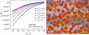
Sb-based halogenated perovskite micro-crystals were obtained, having the shape of ultra-thin hexagonal platelets. These were analyzed multi-parametrically (structural, optical, and electrical). Photoluminescence analysis led to the conclusion that these crystals have light emission. Transistors manufactured on transparent structures having as active layer the halogenated perovskite micro-crystals are characterized by an electrical response predominated by the presence of electrically charged ions.
Articles:
- „Influence of doping the inorganic cation with Eu or Sb on the properties of perovskite films”, Stancu, L.N. Leonat, A. G. Tomulescu, S. Derbali, L. Pintilie, C. Besleaga, A.C. Galca, F. Neatu, S. Neatu, M. Florea, I. Pintilie, Physica Scripta 75 (2020) 7, WOS: 000536270000001;
- „The behaviour of gold metallized AlN/Si and AlN/glass based SAW structures as temperature sensors”, Nicoloiu, G. E. Stan, C. Nastase, G. Boldeiu, C. Besleaga, A. Dinescu, A. Müller, IEEE Transaction on Ultrasonics, Ferroelectrics, and Frecquency Control – accepted
- "Optoelectronic Properties of (CH3NH3)3Sb2I9 crystals" C. Besleaga, I.C. Ciobotaru, V. Stancu, A.C. Galca, I. Pintilie, L. Pintilie - under preparation
- „Ferroelectric field effect transistors based on PZT and IGZO”, Besleaga, R. Radu, L.-M. Balescu, V. Stancu, A. Costas, V. Dumitru, G. Stan, L. Pintilie, Journal of the Electron Devices Society 7 (2019) 268, WOS: 000460753000038.
- „The hysteresis-free behavior of perovskite solar cells from the perspective of the measurement conditions”, A. Nemnes, C. Besleaga, A.G. Tomulescu, L.N. Leonat, V. Stancu, A. Manolescu, I. Pintilie, Journal of Materials Chemistry C 7 (2019) 5267, WOS: 000472443000006.
- „Influence of doping the inorganic cation with Eu or Sb on the properties of perovskite films”, Stancu, L.N. Leonat, A. G. Tomulescu, S. Derbali, L. Pintilie, C. Besleaga, A.C. Galca, F. Neatu, S. Neatu, M. Florea, I. Pintilie, Physica Scripta 75 (2020) 7, WOS: 000536270000001;
- „The behaviour of gold metallized AlN/Si and AlN/glass based SAW structures as temperature sensors”, Nicoloiu, G. E. Stan, C. Nastase, G. Boldeiu, C. Besleaga, A. Dinescu, A. Müller, IEEE Transaction on Ultrasonics, Ferroelectrics, and Frecquency Control – accepted
- "Optoelectronic Properties of (CH3NH3)3Sb2I9 crystals" C. Besleaga, I.C. Ciobotaru, V. Stancu, A.C. Galca, I. Pintilie, L. Pintilie - under preparation
CRISTINA BESLEAGA STAN, PhD in Physics
Senior Researcher II
Department: Laboratory of Multifunctional Materials and Structures
PROJECTS/ NATIONAL PROJECTS
Copyright © 2026 National Institute of Materials Physics. All Rights Reserved